The complete guide to PCB pad :types, size, spacing, repair and
$ 21.50 · 4.9 (648) · In stock

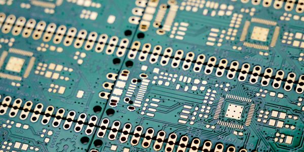
Soldering is one of the most important processes in PCBA processing. On printed circuit boards, electrical connections to all components are made via PCB pads. The PCB pads are a very critical part of the PCB that determines where components are soldered on the PCB.The size, shape, and position of pads in a PCB directly depend on the manufacturing quality of the board. Today we will take a look at the PCB pad in SMT soldering.
Soldering is one of the most important processes in PCBA processing. On printed circuit boards, electrical connections to all components are made via PCB pad.
What are Vias in Pad? Advantages, Limitations, Applications, and Comparison with Conventional Vias

Getting to know PCB terminal blocks : function, material and sizes - IBE Electronics

LG Innotek launched the world's thinnest semiconductor package substrate - IBE Electronics

LG Innotek launched the world's thinnest semiconductor package substrate - IBE Electronics

PCB Pad Size Guidelines: Finding the Proper Pad Sizes for Your Circuit Design

A Comprehensive Guide to Printed Circuit Board Pad - FS PCBA

What is a Pad in PCB Design and Development

PCB connector : definition, types, and how to choose and identify - IBE Electronics

How to solve the solder scooped on welding? - IBE Electronics
How To Repair Damaged /Missing PCB Pads INVISIBLE Fix, 45% OFF
What is Pad to Pad (PP) in PCB ?. Pad to Pad or PP is an important design…, by RayMingPCB
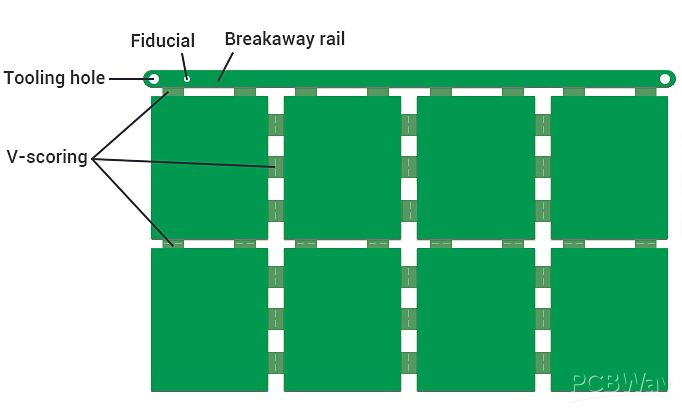
V-Scoring - PCB Prototype the Easy Way - PCBWay

An ultimate guide to PCB gold fingers - IBE Electronics

What is reflow soldering? Technological process, defects and comparison with wave soldering - IBE Electronics

The complete guide to PCB pad :types, size, spacing, repair and comparison - IBE Electronics